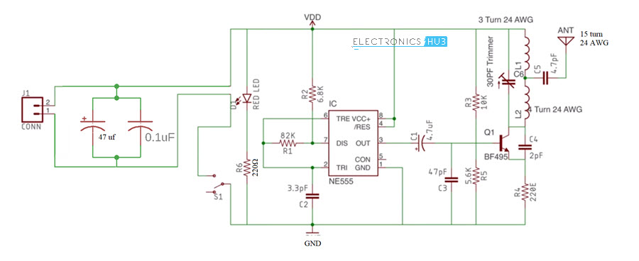
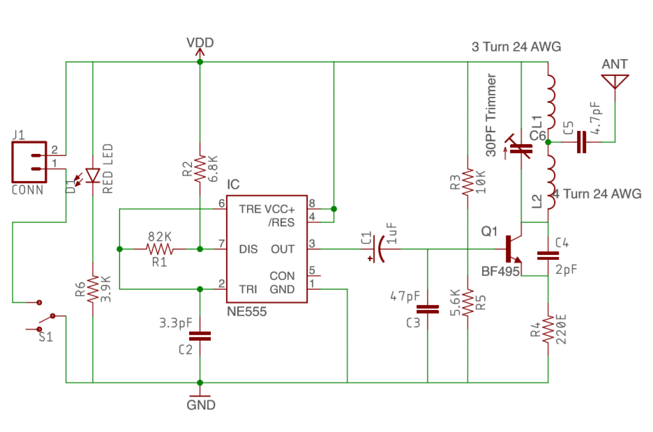
Mobile Jammer Circuit Diagram And Components

How Does A Signal Jammer Work A mobile jammer circuit is comprised of several key components. first, there is the antenna, which is the component that transmits and receives the signal. the antenna is connected to a controller circuit, which processes and adjusts the transmission. then, there is the rf amplifier, which boosts the signal strength. Increase the frequency of tuned circuit by using this formula f= 1 (2*pi*sqrt (l*c)). increase the inductor capacitor circuit components value for increasing the frequency. get guide on mobile phone jammer circuit and its working. this circuit works in the range of 100m. and blocks the signals of cell phones.

Mobile Phone Jammer Schematic Iot Wiring Diagram The use of different frequencies makes it difficult to have a jammer for all frequencies. however, the below mentioned formula can be used to calculate the required values. f = 1 (2*pi*sqrt(l1*c1)) depending on the frequencies you need to block, the values of the inductor (l1) and capacitor (c1) can be altered. Spy pocket mobile phone jammer signal cell network in karol bagh metro station new delhi gadgets id 18661067830. portable rf jammer circuit atmega48 atmega32 avr. pdf the design and implementation of a mobile phone detector device with frequency jamming feature. cell phone signal jammer using 555 ic timer project. is it possible to design a. A mobile jammer is an instrument used to protect the cell phones from the receiving signal. the mobile jammer device broadcasts the signal of the same frequency to the gsm modem. the jamming is said to be successful when the mobile phone signals are disabled in a location if the mobile jammer is enabled. mobile jammer block diagram of mobile jammer. By doing so, these jammers inhibit the transmission of data from cellular phones, preventing the user from making any calls or sending text messages. these jammers work by generating an interference signal in a certain frequency range, and blocking any incoming signals on that frequency range as well.

Full Power Mobile Phone Jammer Circuit Diagram Expert Circuits A mobile jammer is an instrument used to protect the cell phones from the receiving signal. the mobile jammer device broadcasts the signal of the same frequency to the gsm modem. the jamming is said to be successful when the mobile phone signals are disabled in a location if the mobile jammer is enabled. mobile jammer block diagram of mobile jammer. By doing so, these jammers inhibit the transmission of data from cellular phones, preventing the user from making any calls or sending text messages. these jammers work by generating an interference signal in a certain frequency range, and blocking any incoming signals on that frequency range as well. Useful steps. 1) solder the bf494 transistor on the vero board & solder a 22nh inductor to its collector pin. 2) solder a 15nf capacitor on the collector of the bf494 to vcc of the circuit. 3) solder the two 4.7pf capacitors in parallel between collector & emitter of the transistor. 4) solder a 39k ohm resistor & a 102pf capacitor to the base. Circuit diagram and description. figure 1.1 is a circuit diagram of mobile jammer. the inverter is held on the pcb configuration, and the 7th and 14th pins are used for battery connections, with the remaining pins connected internally. the second input and output terminals are attached to a tuning capacitor.

Gsm Signal Repeater Circuit Diagram Useful steps. 1) solder the bf494 transistor on the vero board & solder a 22nh inductor to its collector pin. 2) solder a 15nf capacitor on the collector of the bf494 to vcc of the circuit. 3) solder the two 4.7pf capacitors in parallel between collector & emitter of the transistor. 4) solder a 39k ohm resistor & a 102pf capacitor to the base. Circuit diagram and description. figure 1.1 is a circuit diagram of mobile jammer. the inverter is held on the pcb configuration, and the 7th and 14th pins are used for battery connections, with the remaining pins connected internally. the second input and output terminals are attached to a tuning capacitor.

Comments are closed.